SPI Flash Read Module [Verilog]
Requirement Analysis
This module implements a Flash controller that reads 4 bytes at a time.
As mentioned in Building a Computer with Nexys4 DDR [1]: Hardware, the computer needs a “hard disk” for reading read-only data.
Principle Analysis
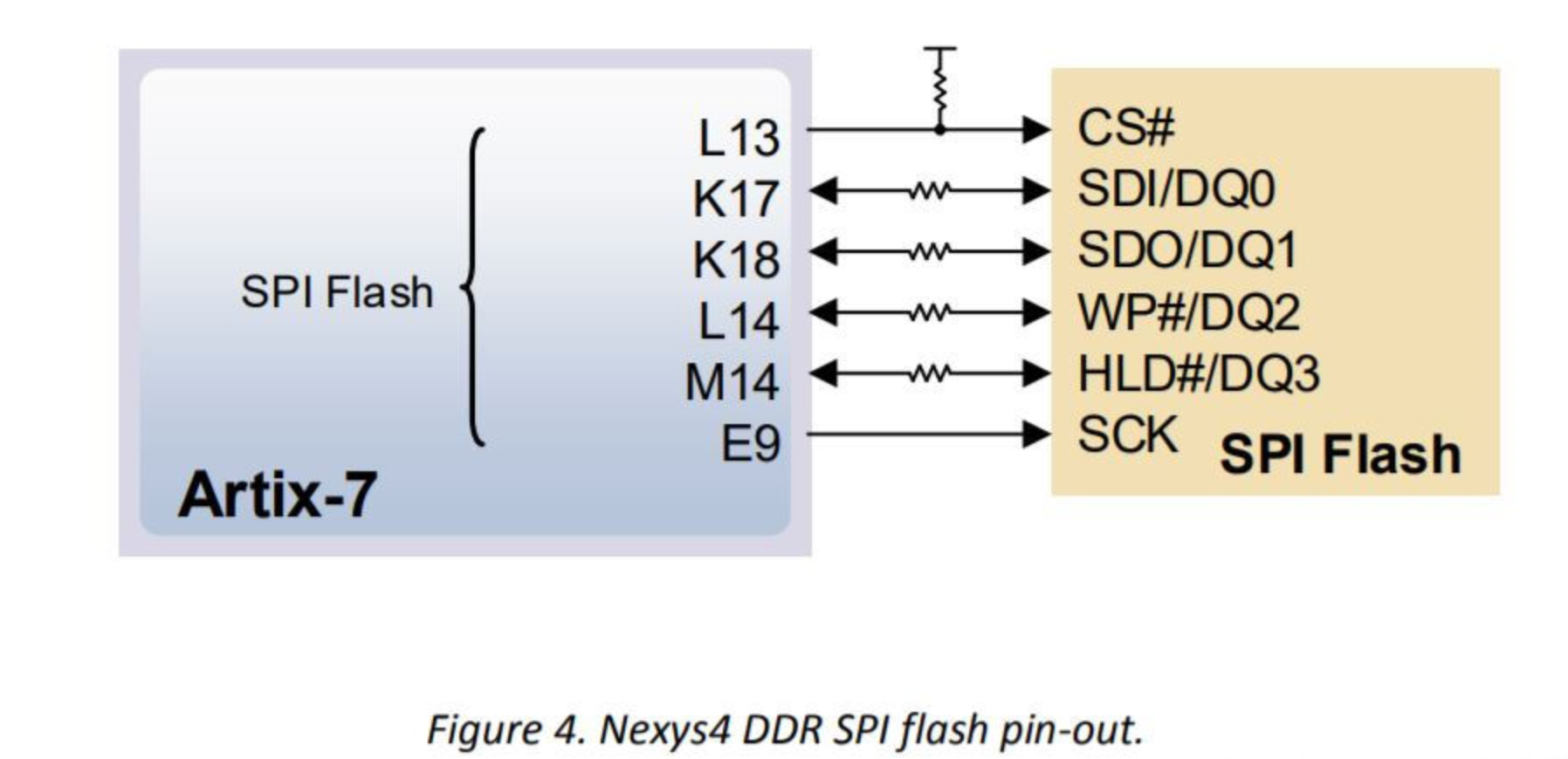
The SPI Flash chip used by Nexys4 DDR is the S25FL128S.
The circuit diagram is below:
What Is SPI?
For simplicity, I only introduce the basics here. For details, see the wiki.
SPI is a serial bus protocol. Data is transmitted bit by bit through a wire. The signals needed here are sck, cs_n, si, and so.
sck is the clock signal, used for synchronization. Its frequency can be chosen freely within the working range.
cs_n is the chip-select signal. The _n suffix means active low, so the chip starts working when cs_n is pulled low.
si is the signal line input to the master device. Reading data from the Flash chip depends on it.
so is the signal line input to the Flash chip. Writing data to the Flash chip depends on it.
What Is a Flash Chip?
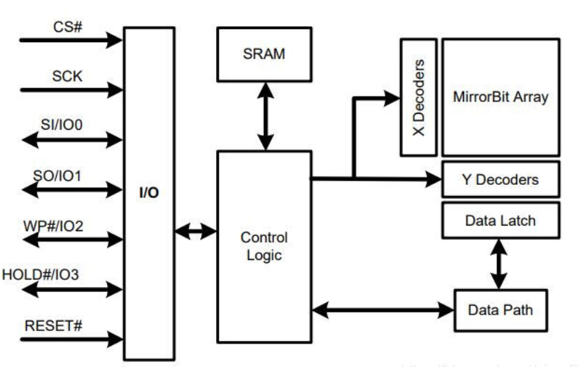
Simply put, it consists of many readable and writable cells, EEPROM, plus a controller. The controller wraps many commands for operating those cells. So the most important part of using a Flash chip is sending the correct commands to its controller.
The structure of the Flash chip is shown below:
Flash commands vary slightly across manufacturers, but because there are standards, most common commands are the same. You can refer to each chip’s documentation.
Timing
Flash Chip Timing
Since we only need to read data, this article only introduces the one command used here: READ.
According to the S25FL128S documentation, the timing of the read command is:
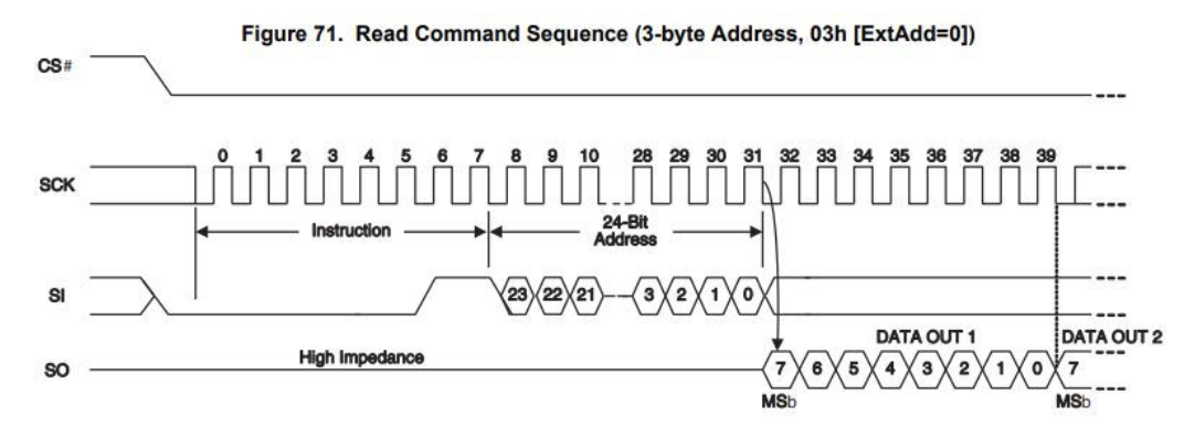
From the diagram, to read data we need to:
- Pull
cs_nlow. - Keep
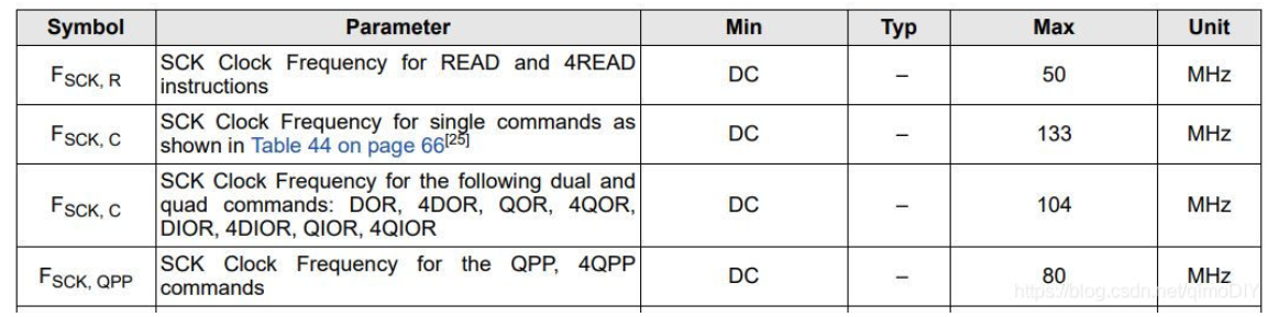
sckwithin the working frequency range. The datasheet says the maximum frequency for theREADcommand is 50 MHz, sosckcan be anywhere in(0, 50M]. Since the onboard crystal of Nexys4 DDR is 100 MHz, 50 MHz is convenient to generate by division.
- Send the
READcommand,03H, and the 24-bit address bit by bit through thesosignal line. - Finally, the Flash chip outputs data bit by bit through the
sisignal line.
Wishbone Bus Read Timing
As a peripheral, the Flash controller needs to connect to the bus, so the interface must satisfy the bus requirements.
This computer uses the Wishbone bus. Its timing is relatively simple. Here is the signal flow for a bus read operation:
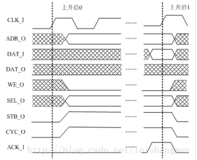
In short, during operation, STB_O and CYC_O are raised at the same time, the address is put into ADR_O, and then the circuit waits for clock cycles on CLK_I. The bus then waits for the peripheral. When the peripheral finishes processing the signal, it raises ACK_I to complete the transfer.
After the master receives the data, it lowers STB_O and CYC_O. At that point, the peripheral knows that the access is complete and lowers ACK_I.
Design
State Machine Design
This part mainly refers to this article.
As shown below: