DDR2 RAM Read/Write Module [Verilog]
Requirement Analysis
Building a Computer with Nexys4 DDR [1]: Hardware needs memory with a minimum read/write width of 8 bits and a maximum read/write width of 32 bits.
Principle Analysis
The DDR2 SDRAM on the Nexys 4 DDR is the MT47H64M16HR-25:H. Its datasheet is here.
Because the DDR protocol is relatively complex, Xilinx provides a memory-controller IP core that simplifies DDR control: Memory Interface Generator, or MIG. This module uses that IP core.
DDR RAM Timing
It has the following signals:
app_addr [26:0] in: data address
app_cmd [2:0] in: operation command, 3'b001 for read and 3'b000 for write
app_en in: command enable
app_rdy out: command accepted; SDRAM raises it after receiving the signal
app_wdf_data [127:0] in: write data, written into SDRAM after being processed by app_wdf_mask
app_wdf_mask [15:0] in: each bit corresponds to one byte in the write data; setting a bit high means ignoring that byte when writing to SDRAM
app_wdf_end in: raised when sending the last data item, to notify SDRAM that the write operation is ending
app_wdf_wren in: write enable; after app_wdf_data and app_wdf_mask are prepared, raise this signal to tell SDRAM it can start writing
app_wdf_rdy out: write-data command accepted; SDRAM raises it after receiving app_wdf_data and app_wdf_mask
app_rd_data [127:0] out: read data
app_rd_data_valid out: read data valid; SDRAM raises it when data has been read into app_rd_data
app_sr_req in: reserved pin, should be pulled low
app_ref_req in: raise this signal for one clock cycle to send a refresh command to DRAM
app_zq_req in: raise this signal for one clock cycle to send a ZQ calibration command for ODT resistance calibration
app_sr_active out: reserved pin
app_ref_ack out: raised when SDRAM responds to the refresh signal
app_zq_ack out: raised when SDRAM responds to ZQ calibration
ui_clk out: user clock provided by the IP core; sequential logic operating this IP core must use this clock
ui_clk_sync_rst out: reset signal for user logic; same as above, sequential logic operating this IP core must use this clock domain
Wishbone Bus Write Timing
Since this is memory, it must support writes. The diagram below shows the Wishbone bus timing for write operations. Read timing was already introduced in the previous Flash article.
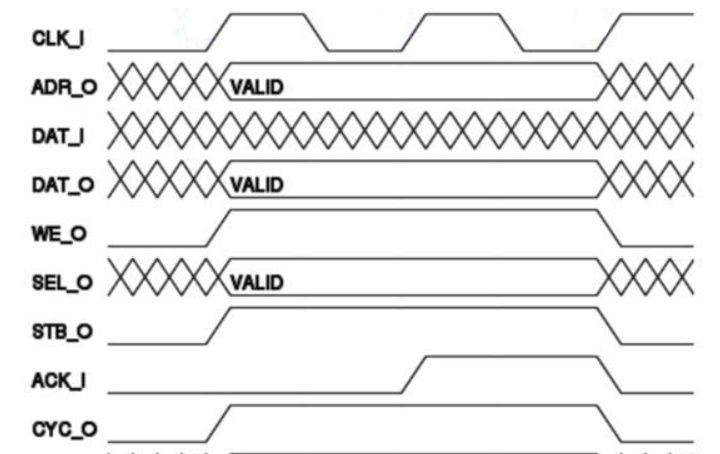
When the CPU needs to write to memory, it raises STB_O, CYC_O, and WE_O, and provides ADR_O and DATA_O. When memory sees STB_O and CYC_O high, it starts the operation. After the operation finishes, it raises ACK_I.
The Wishbone bus controller receives the ACK_I signal, notifies the CPU, and lowers STB_O and CYC_O. Then the memory returns to the waiting-for-command state.
Design
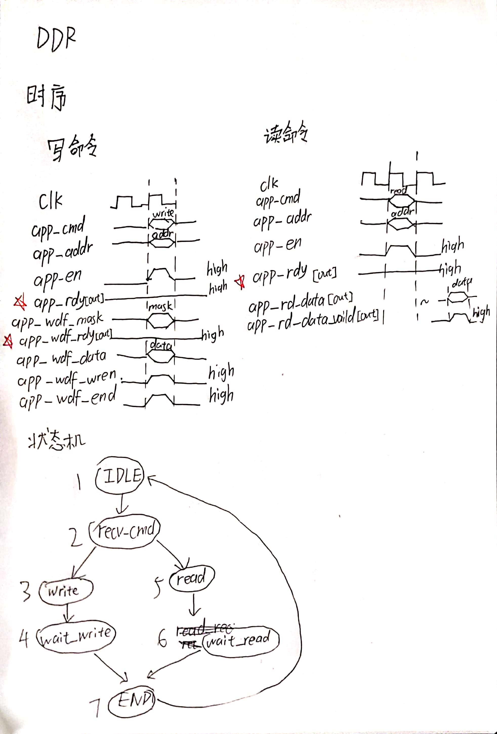
Timing and State Machine Design
As shown below:
Reference Links
DDR2 simulation and design on Nexys4 DDR
FPGA basics [9]: accessing external DDR2 memory on a development board
Using the DDR controller MIG core
DDR read/write control in Vivado MIG